Nanostructured III-V compound semiconductors
Prof. Dr.-Ing. Markus-Christian Amann
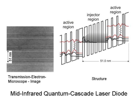
The research activities in this group are concentrated on modern technologies for III-V compound semiconductors and their use for developing advanced electronic and optoelectronic devices. This comprises the development of epitaxial, patterning, micro- and nanostructuring, etching and coating techniques as well as the design and fabrication of semiconductor laser diodes and other nanophotonic components. The applied material systems are GaAs-AlGaAs, InGaAsP-InP and antimonide based compounds that are grown with molecular beam epitaxy (MBE), chemical beam epitaxy (CBE) and metal-organic vapour-phase epitaxy (MOVPE) with an accuracy on the atomic scale. Lateral device structuring in the sub-100-nm-range is obtained by using electron-beam lithography. Reactive ion etching enables the well-defined processing of the various devices with a high material selectivity of the etching rate. The group is also well equipped with evaporation and sputtering techniques for passivation and contacting of the devices. Among the key devices investigated are single-mode and wavelength-tunable laser diodes for the wavelength range between 1.3 and 3µm using InP- and GaSb-based compounds, InGaAsP and AlInGaAs vertical cavity surface-emitting laser diodes in the 0.8-2µm wavelength range, and microcavity light-emitting devices in the 2-5µm regime. Novel material concepts are employed for new functionalities, such as InAs quantum dots on GaAs for vertical cavity surface-emitting lasers as well as 1D, 2D and 3D photonic crystal structures for the complete mode control in semiconductor light sources.
