Diamond surface nano electronics
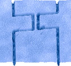
Hydrogen-terminated surfaces of single-crystalline diamond have generated a lot of interest due to their surprising electronic properties. Whereas “normal“ diamond with oxygen termination is an almost perfect insulator, hydrogen termination of diamond crystals by a simple plasma process gives rise to a negative electron affinity, meaning that electrons in the diamond conduction band have a higher energy than electrons in vacuum. One important consequence of this fact is that hydrogen-terminated diamond samples in contact with air spontaneously form a two-dimensional hole gas via electron transfer from the diamond crystal to adsorbed hydronium (H3O+) molecules at the surface. This hole gas is located directly at the diamond surface and exhibits a metallic character with hole densities up to 1014 cm-2. Surface electronic devices can be defined via a simple local oxidation, which creates highly resistive barriers between the metallic hydrogenated regions. As an example, the figure below shows an in-plane-gate transistor (IPGT), which was obtained by electron beam lithography. Such transistors are particularly interesting for diamond sensor devices.


In-plane-gate transistor obtained by local oxidation of a hydrogen-terminated diamond surface. The left picture shows the basic outline of the device. On the right side, an AFM micrograph of the e-beam lithography mask for the channel region is depicted. The width of the dark insulating lines is below 100 nm, the channel width is about 50 nm.