Ultrafast transport current in GaAs based photoswitches
Prof. Dr. Alexander Holleitner
Commercial sources and detectors for terahertz electromagnetic radiation (THz-EMR) have lead to numerous applications in materials and life sciences. Nevertheless, the physical processes involved in THz-EMR generation are still subject of fundamental research. For instance, THz-EMR is generated by a non-linear wave conversion of a short laser pulse in an electro-optic medium, by the photoelectric effect of a surface built-in electric field, and by photo-Dember mechanisms. Furthermore, hot carrier dynamics and collective electron-hole plasma processes can be probed by analyzing the emitted THz-EMR from a semiconductor test structure.
THz-EMR can also be generated in photoswitches (PS). These are semiconductor slabs which are voltage-biased across two surface metal electrodes. The PS is typically excited by an optical femtosecond pulse. In turn, a short current response in the PS leads to THz-EMR. The optical illumination profile determines which optoelectronic phenomenon dominates the current response within the PS. A spatially uniform illumination of the PS gives rise to a transport current pulse, which is limited by the lifetime of the optically excited charge carriers. Since sub-picosecond carrier lifetimes can be achieved in a variety of materials (e.g. GaAs, Si, InGaAs), this kind of THz-EMR generation is widely exploited in scientific and technological applications. A non-uniform illumination leads to a dominating displacement current pulse whose duration can be shorter than the carrier lifetime. While a theoretical description of both mechanisms has been developed, the actual real-space motion of the transport current pulse has not been experimentally characterized so far.
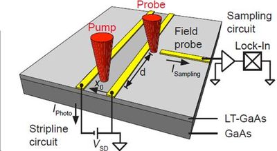
We reported on space- and time-resolved photocurrent studies of a PS [1]. The PS is part of a coplanar stripline circuit (Fig. 1). An optical probe-pulse is focused at a position x0 in between the two CPS. Hereby, the two metal strips of the CPS form a PS for the stripline circuit (Fig. 1). After optical pump-excitation, an electro-magnetic pulse starts to propagate along the CPS. At a distance d, the field-probe of the sampling circuit is short-circuited by an optical probe-pulse for the duration of the lifetime of the photo-generated charge-carriers in the LT-GaAs at this position. The transient electric field of the CPS located at the field-probe during this time-period drives the current ISampling in the sampling circuit (Fig. 1). Most importantly, varying the time-delay ∆t between the optical pump-pulse and the probe-pulse gives access to the time evolution of ISampling = ISampling(Δt).

Fig. 2(a) depicts ISampling as a function of Δt for varying x0. We observe two peaks of ISampling. For all x0, we observe that the first peak occurs at the same ∆t, and we interpret it to result from a displacement current in the PS. Fig. 2(b) shows the schematic of the bandstructure along x0. The optical pump-pulse excites charge carriers at position x0. Before illumination, the electric field |F| = VSD / d is constant in between the two contacts. The excitation laser generates a high local electrical conductivity in the vicinity of x0. Therefore, the electric field drops to zero at the position x0 directly after laser excitation [dashed line in Fig. 2(c)], while it increases in the remaining area to sustain the applied bias VSD. The resulting displacement current density is given by jD =εGaAsε0 δF/ δt. The second peak in Fig. 2(a) is found to shift in Δt with respect to the first peak as a function of x0. The difference of the center positions t12 of the two peaks versus x0 is shown in Figure 2(d).

A linear fit allows us to deduce propagation velocities of ~108 cm/s. This value exceeds typical Fermi- and quantum velocities of single-particle charge excitations in GaAs at the utilized ELaser. However, they are consistent with values for collective electron-hole plasma excitations within a GaAs PS. We therefore conclude that a collective excitation of an electron-hole plasma and not single charge-carriers dominates the transport current on ultrafast timescales in GaAs photoswitches.
Our results suggest that the presented ultrafast transport current phenomena may occur in further GaAs based optoelectronic circuits comprising e.g. nanowires [2,3] and quantum wires [2].
This work is supported by DFG-project HO 3324/4, the German excellence initiative via the "Nanosystems Initiative Munich" (NIM), and the “Center of NanoScience (CeNS)” in Munich.
[1] L. Prechtel, S. Manus, D. Schuh, W. Wegscheider, A.W. Holleitner, Appl. Phys. Lett. 96, 261110 (2010)
[2] S. Thunich, L. Prechtel, D. Spirkoska, G. Abstreiter, A. Fontcuberta i Morral, and A. W. Holleitner, Appl. Phys. Lett. 95, 083111 (2009)
[3] C. Rossler, K.-D. Hof, S. Manus, S. Ludwig, J. P. Kotthaus, J. Simon, A. W. Holleitner, D. Schuh, and W. Wegscheider, Appl. Phys. Lett. 93, 071107 (2008)
[4] K.-D. Hof, C. Rossler, J.P. Kotthaus, A.W. Holleitner, D. Schuh, W. Wegscheider; Phys. Rev. B 78, 115325 (2008)