Photocurrent and photoconductance properties of a GaAs nanowire
Prof. Dr. Alexander Holleitner
Semiconductor nanowires have attracted considerable attention for the past few years because of their compelling electronic, mechanical and optical properties. We investigated the optoelectronic properties of photodetectors based on single p-doped GaAs nanowires. The nanowires are electrically contacted to gold electrodes using a versatile focused ion beam (FIB) deposition technique [1,2]. We experimentally identified two dominating optoelectronic processes in the nanowire photodetectors by measuring the optoelectronic response of the devices as a function of voltage, modulation frequency, photon energy, spatial coordinate, and the polarization of the laser field. On the one hand, a photocurrent is generated at the Schottky contacts between the GaAs nanowires and the metal source-drain electrodes. On the other hand, we observed a photoconductance effect, when illuminating the GaAs nanowire far away from the contacts. We interpret this photoconductance effect to arise from band bending effects caused by surface states on the nanowire surface. In particular, optically generated excess electrons are trapped at the surface, where they act as a negative gating voltage on the p-doped nanowires (photogating effect) [3]. At the same time, the optically excited free excess holes raise the Fermi-energy of the hole gas within the nanowires (photodoping effect) [4]. We demonstrated that the corresponding optoelectronic responses of the nanowires are sensitive to the orientation of linear polarized light. Hereby, the metal-GaAs nanowire-metal circuits act as polarization-sensitive photodetectors, which can be integrated into electronic circuits by the FIB-deposition technique in a very versatile way.

The circuit in Fig. 1(a) features three positions I, II, and III. At position I and III, Schottky contacts between the nanowire and the gold electrodes can be assumed. At position III, however, the nanowire is covered by an opaque carbon layer with a thickness of ~350 nm. At position II, the nanowire is freely suspended. Hereby, the circuit allows locally addressing the optoelectronic processes in the middle of the nanowire independently from the ones occurring at the metal-semiconductor contact. We acquired photocurrent images of the nanowire circuit by recording the photocurrent response IPHOTO at a finite source-drain bias VSD, while scanning the laser spot laterally across the sample. As can be seen in Fig. 1 (b) a dominating contribution of |IPHOTO| occurs at position I compared to |IPHOTO| at position II.

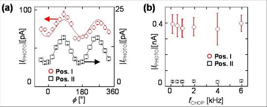
The observed photoconductance and -current signals depend on the polarization of the exciting laser field for both positions I and II [Fig. 2(a)]. The signals follow a cosf dependence, where f is the angle between the wire and the light polarization. We observe that the polarization ratio larger at position II (~ 35 %) than close to the Schottky contact of position I (~ 15 %). In order to test the response time of the metal-nanowire-metal photodetector, we measure IPHOTO of the devices as a function of fCHOP [Fig. 2(b)]. For both positions I and II, we do not detect any dependence of IPHOTO on fCHOP for frequencies between 0.1 and 6 kHz. This reveals that the effects causing the photocurrent and the photoconductance occur on a timescale shorter than ~ (6 kHz)-1 = 167 μs.
This work is supported by the DFG Grant No. Ho 3324/4, the German Excellence Initiative via the “Nanosystems Initiative Munich (NIM),” Marie Curie Excellence Grant SENFED, and the Swiss National Science Foundation (Grant No. 2000021-121758/1) as well as the “Center for NanoScience” (CeNS) in Munich.
[1] C. Ruppert, S. Thunich, G. Abstreiter, A. Fontcuberta i Morral, A. W. Holleitner, M. Betz, Nano Lett. 10, 1799 (2010)
[2] S. Thunich, L. Prechtel, D. Spirkoska, G. Abstreiter, A. Fontcuberta i Morral, and A. W. Holleitner, Appl. Phys. Lett. 95, 083111 (2009)