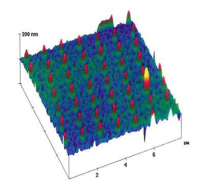
Nanostructuring of semiconductors by laser holography
We use single pulses of a high power ns-laser to generate nanostructures on and in semiconductors. Periodic line and dot patterns are obtained by the interference of two or three coherent laser beams, more complex structures can be generated with digital holograms. Using the third harmonic of a Nd:YAG laser with a wavelength of 355 nm, feature sizes below 50 nm and periods down to 150 nm can be generated over large areas. The use of a single laser shot in combination with holography has the advantage of being insensitive to sample vibrations and is also applicable to non-flat surfaces. This method has been successfully applied to the nanostructuring of amorphous and crystalline silicon, GaAs/AlGaAs heterostructures, GaN, and transparent conductive oxides. Potential applications are grating couplers for solar cells, seed arrays for crystallisation and anodic oxidation, and the realization of templates for nanowires and quantum dots.
